There are the 4 possible values for a component's side:

When you are drawing a single side PCB, you can only draw "1", "2" or "2 SMD" side components. Indeed, in a single side PCB there is no copper in the "blue" side.
You can turn the component in two ways:
- enter the angle in the text box;
- use right mouse button (90� step); SHIFT key reverse rotation direction, CTRL key use 45� step and ALT key use 1� step.
You can increase or decrease component pads size; when you clic on the pad size textbox the next window appears:

When you have entered all the parameters, simply place the component with a left mouse clic:


If the component is stretchable, you have to clic 2 times:


|
To draw tracks, clic on the "track" icon:
The related tool box will appear:

You can enter track width and choose track side.
A single side PCB can only have CU1 side track.
Clic with the left button to start a track and add nodes:

Use the right button to end a track, that is to say, to set the last node:

CU1 side tracks are black, CU2 side tracks are light blue:

|
To place a copper text, clic on Edit / Insert copper text� menu, or hit CTRL + W. The following window appears:

You can enter a text or choose a text from PCB's extra information; in this case, when you change extra PCB information, the copper text will be updated.
Once you have clic OK, you can rotate and place the copper text with mouse like a component:

|

|
You can check the "Layers / Always display no splited text" menu to read easily all coppers text, but display is not WYSIWYG.
|
CiDess has a high number of display parameters.
"Zoom" and "Grid" menus
"Layers" menu
"Display" menu
"Display - Advanced settings" menu (new in CiDess III)
"Zoom" and "Grid" menus
In "Zoom" menu you can choose one of the four zoom levels.
In "Grid" menu you can choose grid step. Indeed, mouse cursor has not continuous motion but it follows grid's nodes.
|
|
|
A 50 mil step is suited to drawing with standard components types.
Use 10 or 5 mil step with components types which have pads with non-standard alignment.
|
"Grid" menu allows you to show or hide the grid and change grid's origin.
Pointer's coordinates are displayed at the right of the display tool bar:

|
|
|
"Zoom" and "Grid" menu appears as popup menus when you clic on the display tool bar.
|

"Layers" menu
|
|
|
New in CiDess III: Hidden objects cannot be selected, moved or modified. |
It allows you to show or hide layers.
There are four layers:
- CU1 is the copper on copper side
- CU2 is the copper on components side (don't exist on single sided PCB)
- SOL is the solid shape layer
- TXT is the text layer.
In the sub menu "Displayed solid" you can choose to show all solids or solids that are visible on side 1 or side 2. If you design a PCB with a
high number of components in both sides, display parameters allow you to view only things that are visible on side 1 or on side 2:
All:

Side 1:

Side 2:

In the sub menu "Displayed text", you can choose to show name and value, name only or value only.
In the sub menu "Text size" you can set the font size.
You can choose to display text with transparent or white background.
|
|
|
If you clic on CU1, CU2, SOL et TXT in the display toolbar you can show or hide layers.
Use the right mouse button on TXT, you can choose the text to display.
New in CiDess III: Use the right mouse button on SOL, you can choose the solid to display.
|

"Display" menu
"Show mouse's line" sub menu allows you to show or hide the cursor lines.
"Selection tolerance" sub menu allows you to set up cursor accuracy in "Multiple selection" and "Pointer" mouse mode. It's an important parameter; if it is badly adjusted you will met problems to select elements with mouse.
"Nomenclature" sub menu show components list:

"Check component names..." sub menu allows you to verify if there are no two or more components that have the same name:

"3D view" sub menu launch 3D view utility.
Check the "Use zoom for preview" menu to use the same zoom level for the whole PCB and component types preview. It's useful when browsing small component types.
"Display - Advanced settings" menu
The following window appears:

You can set screen scale and every colors used.
|
|
Modify an element with the pointer
|     
|
To edit an element with mouse pointer, clic on the mouse pointer icon.
The related tool box will appear:

The displayed text explains all pointer mode facilities.
|
|
|
If you met problems to select an element, go in "Display" menu and adjust "Selection tolerance" parameters.
Use right mouse button to ignore tracks so components selection is easier.
|
The next picture shows what's happen when you clic on a component:

The next picture shows what's happen when you clic on a stretchable component's pad:

The next picture shows what's happen when you clic on a component while pressing SHIFT key:

The next picture shows what's happen when you clic on a track:

The next picture shows what's happen when you clic on a track's node:

The next picture shows what's happen when you clic on a track's node while pressing SHIFT key:

|
|
|
If you just want to edit a component or a track, use pointer mouse mode (see previous paragraph).
|
To do group operations, clic on the selection icon.
The related tool box will appear:

"+GP1" "+GP2" "-GP1" "-GP2" buttons are related to ground plane pads and tracks, see next paragraph.
There are two ways to select elements:
- One by one
- With a select rectangle
In the first case, you have to select components and tracks one by one with mouse. Selected elements become lighter:

To unselect an element, clic again on it.
|
|
|
If you met problems to select an element, go in "Display" menu and adjust "Selection tolerance" parameters.
|
In the case of rectangular selection, you have to draw a rectangle; all elements contained in the rectangle are selected.


It's possible to add several selections.
Elements stay selected until they are unselected by user.
Once you have select elements, you can:
- Cut them
- Copy them
- Delete them
- Move them
Also the tool bar has the "Paste" command.
|
|
Group operations 2/2: Tracks and pads merged with ground plane
|
|
When printing or saving PCBs, you have the possibility of making a ground plane.
CiDess allows you now to select tracks and pads to merge with a ground plane side CU1 and/or CU2.
Tracks and pads merged with a ground plane display with specific colors which you can choose in the menu "Display - Advanced settings".
Here is an example:

Both images at the top show a normal circuit and the PCB with ground plane.
Both images below show a circuit among which certain tracks and pads (orange) are merged with the ground plane CU1, and the obtained PCB.
It is possible, for the CU1 and CU2 ground plane, to select tracks and pads which will be merged with.
Click on the selection icon; the related tool box will appear:
"+GP1" button allows you to merge selected elements with CU1 ground plane.
"+GP2" button allows you to merge selected elements with CU2 ground plane.
"-GP1" button allows you to remove selected elements from CU1 ground plane.
"-GP2" button allows you to remove selected elements from CU2 ground plane.
Here is an example:
Select one (or several) track connected electrically to the list of tracks and pads which you wish to merge with a ground plane:

Then, click the "+GP1" button; CiDess then fetches all the parts of the circuit linked electrically (CiDess also takes into account straps) to the elements that you selected and mark them as merged with the ground plane:

Obviously, we can merge with the CU1 ground plane only CU1 tracks and with CU2 ground plane only CU2 tracks. Only pads of non-SMD components can be merged with both ground planes.
|
|
|
You can use "+GP1" and "+GP2" and then "-GP1" and "-GP2" buttons to check which parts of the circuit are electrically connected with the others - it is all the more useful as CiDess take into account straps for the selection; on the other hand CiDess does not manage circuits passing as a face to the other.
|

|
Nothing prevents you from merging with ground plane different parts of the circuit which are not already connected electrically together. This is a BAD PRACTICE because it is possible that during the creation of the PCB, the ground plane connects or does not connect electrically these two parts. Furthermore if the PCB is realized without ground plane, these parts will remain insulated.
|
|
|
A GOOD PRACTICE consists in connecting at first electrically with tracks and straps all the parts of the circuit which you want to merge with a ground plane. So, you are certain that all these parts will remain connected electrically together whatever the way the PCB is created.
|
|
|
Nothing prevents you from creating voluntarily two or several insulated ground planes on the same face. You have to be all eyes during the creation of the PCB; do not hesitate to place explanations with copper texts or in the documentation of your project.
|
|
|
If you often draw the same structure (for example a 7805 supply) this function allows you to save a lot of time. You just have to save the structure in a file. Then, when you draw a PCB, instead of drawing the structure each time, you simply have to insert the previous file.
|
Export PCB in 3DG 3D format
You can save a PCB in 3DG format.
In "File" menu choose "Create 3DG file...".
This file format is supported by a lot of 3D software.
Export PCB in STL 3D format
You can save a PCB in STL format.
In "File" menu choose "Create STL file...".
This file format is supported by a lot of 3D software.
VisCAM View free software allows you to view CiDess' STL file in color, make measures, and create pictures.
Export PCB in GIF or BMP format
GIF file format allows you to save a big size picture in a small file, without quality loss.
In "File" menu choose "Save PCBs as GIF or BMP files...".
The next window will appear:

Tool tip texts and a WYSIWYG sample help you to choose right parameters.
CiDess III allows you to print normal or negative copper text if the PCB is printed with a ground plane.
With CiDess III.2, you can save files in BMP format.
This function is useful to send your PCB or if you have to print PCB on a computer without CiDess.
|
|
|
If you want to print GIF files, choose a high zoom value (a least 4).
|
Export layout in GIF or BMP format
You can save the layout as GIF file.
In "File" menu choose "Save picture as GIF or BMP file...".
The next window will appear:

Copy image to clipboard
In "Edit" menu choose "Copy picture".
Current picture is copied in clipboard. It's available for other programs (word processor, graphic software).
|
CiDess allows you to print PCB, layout, and PCB's information.
In the "File" menu choose "Print PCB(s)..."
The next window will appear:

Tool tip texts and a WYSIWYG sample help you to choose right parameters.
You can also print normal or negative copper text if the PCB is printed with a ground plane, and have page setup feature:


|
|
|
Check if your PCB is printed at the right scale and right way before starting the exposure.
|
In the "File" menu choose "Print layout...".
The next window will appear:

New in CiDess III: In the "File" menu choose "Print PCB information...".
The next window will appear:

To view a PDF sample of a printing, clic here.
|
|
PCB milling with a CNC machine (CiDess 4 - Depreciated) |
|
This function is depreciated and has changed un CiDess 4.25. See next paragraph.
CiDess 4 allows you to create a special BMP picture to mill the PCB with third party CNC software (like BTP4M).
Mill means both drill pad's holes and etch tracks' paths
Notice that CiDess can directly generate GCODE for drilling a PCB before or after chemical etching, as shown in the next part of this manual.
|
|
Before milling a PCB, check it! You can print the PCB at real size and then place the components on the sheet. |
How it works? CiDess create a picture for the side you want to mill, with special colors corresponding to
- areas to drill (CoulPercage)
- areas to etch, copper inside will be removed by machining (CoulCuGrave)
- areas to deep-etch, the machine will trace an etch line around (CoulCuDetoure)
You can choose these three colors and the backcolor (CoulCuIntact) in the "advanced settings" in the "display" menu.
The next picture shows how the CNC software had to use the colors in the BMP picture:

On top of the picture, with blue, gray and red rectangles and circles, the small black disk figures a CNC machine milling tool. Dot lines are tool paths. White background is CoulCuIntact color.
The bottom of the picture shows the result of the rectangles milling operation on a real PCB (bakelite is in brown, and copper in orange).
In the CoulCuDetoure and CoulCuGrave cases, the tool only etch PCB's copper surface; with CoulPercage, the tool mills the whole depth of the PCB.
CiDess offers you several parameters to create BMP pictures, allowing you different milling ways.
In file menu, clic on "Create BMP picture for CNC milling...". The following window appears:

Three preview pictures at the left helps you to understand how it works.
In the next screenshots, the colors were like the following:
- CoulCuGrave = Black
- CoulCuDetoure = Blue
- CoulPercage = Red
- CoulCuIntact = White
First preview picture shows the CiDess' editor PCB style.
Second preview picture shows the BMP picture's style
Third preview picture shows how the PCB will be machined; remaining copper is in black, etching is in white.
Here is different screenshots:


|
|
|
If your PCB is 2-sided, in other words if it's contain tracks or SMD components on side 2, you have to mill your PCB in two steps, so you have to create one BMP file for each side. In this case, it's useless to drill again the holes when machining side 2; this isn't even recommended because clamping tolerance can cause twist drill breaking or makes holes oval. To avoid those problems, when create the BMP picture for side 2, enabled the "No drill" function.
|
|
|
If your PCB has notches or cuts inside, you can open the BMP file with a drawing soft and draw notches and cuts with the CoulPercage color.
Warning: the color has to be exactly the same that CoulPercage, and you have to disable all antialiasing functions of the drawing software.
|
|
|
You can had an etched logo on the PCB; just open the BMP file with a drawing soft and draw the logo with CoulCuGrave, CoulCuIntact or CoulCuDetoure color.
Warning: the color has to be exactly the same that CoulCuGrave, CoulCuIntact or CoulCuDetoure, and you have to disable all antialiasing functions of the drawing software.
|
|
|
In the user manual of your third party CNC picture milling software, you can find useful information. For example, BTP4M software allows you to draw with a special color the external shape of the PCB. So you can mill PCB with cloud shape, X-mas tree shape, star shape...
Warning: the color has to be exactly the same that specified in the CNC software's manual, and you have to disable all antialiasing functions of the drawing software.
|
CiDess offers you to create an extra info file. This extra file will have the same filename that the BMP file, but with .BMP.TXT extension. It contains useful data as PCB real size and the colors used by CiDess. BTP4M software can read this file, so it's strongly recommended to leave enabled this function.
|
|
|
Be carefully if you edit BMP files with a drawing software. Do no use other colors than CoulCuGrave, CoulCuPercage, CoulCuDetoure, CoulCuIntact and colors specified in the CNC software's manual. You have to disable all antialiasing functions of the drawing software, otherwise it will draw shaded off color pixels. For the same reason, do not resize a BMP file, and only use BMP file format without compression. |
|
PCB milling with a CNC machine |
|
CiDess 4 allows you to create a special BMP picture to mill the PCB with third party CNC software (like LUCAS-CNC-BMP).
Mill means both drill pad's holes and etch tracks' paths
Notice that CiDess can directly generate GCODE for drilling a PCB before or after chemical etching, as shown in the next part of this manual.
|
|
Before milling a PCB, check it! You can print the PCB at real size and then place the components on the sheet. |
How it works? CiDess create a picture for the side you want to mill, with special colors corresponding to
- areas to drill (CoulPercage)
- areas to etch, copper inside will be removed by machining (CoulCuGrave)
You can choose these three colors and the backcolor (CoulCuIntact) in the "advanced settings" in the "display" menu.
CiDess also use CoulPercage for cutting the border of the PCB, if you want your NC machine cut your PCB.
In other words, each color corresponds to a machining depth:
- CoulCuIntact: zero depth, the circuit is intact;
- CoulCuGrave: intermediate depth, only the copper layer is removed;
- CoulPercage: full depth, the whole PCB is milled.
CiDess offers you several parameters to create BMP pictures, allowing you different milling ways.
In the next screenshots, the colors were like the following:
- CoulCuGrave = Black
- CoulPercage = Red
- CoulCuIntact = White
In file menu, clic on "Create BMP picture for CNC milling...". The following window appears:

Three preview pictures at the left helps you to understand how it works.
If your PCB is 2-sided, in other words if it's contain tracks or SMD components on side 2, you have to mill your PCB in two steps, so you have to create one BMP file for each side. In this case, just check the both checkboxes "Side 1" and "Side 2"; CiDess will generate the two pictures you need. In this case, drills and border cut are made only in one side (it's useless to drill again the holes when machining the other side; this isn't even recommended because clamping tolerance can cause twist drill breaking or makes holes oval).
|
|
|
If your PCB has notches or cuts inside, you can open the BMP file with a drawing soft and draw notches and cuts with the CoulPercage color.
Warning: the color has to be exactly the same that CoulPercage, and you have to disable all antialiasing functions of the drawing software.
|
|
|
You can had an etched logo on the PCB; just open the BMP file with a drawing soft and draw the logo with CoulCuGrave or CoulCuIntact color.
Warning: the color has to be exactly the same that CoulCuGrave or CoulCuIntact, and you have to disable all antialiasing functions of the drawing software.
|
With each BMP file, CiDess will create extra info files, which have the same filename that the BMP file, but with ".BMP.BTi" extensions:
- file.BMP.BT1 : picture color code;
- file.BMP.BT2 : path recognition and smoothing parameters;
- file.BMP.BT4 : picture scale;
- file.BMP.BT5 : hole recognition and machining depths.
These files are useful if you use the LUCAS-BMP-CNC software to machine your PCBs.
|
|
|
Be carefully if you edit BMP files with a drawing software. Do no use other colors than CoulCuGrave, CoulCuPercage, CoulCuIntact and colors specified in the CNC software's manual. You have to disable all antialiasing functions of the drawing software, otherwise it will draw shaded off color pixels. For the same reason, do not resize a BMP file, and only use BMP file format without compression. |
|
PCB drilling with a CNC machine |
|
This function has been removed since CiDess 4.27 - In practice, precise positioning of the PCB in the milling machine was too difficult. Use another software, such as LUCAS-BMP-CNC to drill AND mill the circuit, to punch holes before drilling, to manage clamping...
CiDess can directly generate GCODE to drill a PCB with a CNC machine. The PCB can be drilled before or after etching.
|
|
Before drilling a PCB, check it! You can print the PCB at real size and then place the components on the sheet. |
|
|
Before using this function, please carefully read your CNC machine�s manual. |
In "File" menu, clic on "Drill PCB with CNC machine...". The following window will appear :

� << Previous � and � Next >> � buttons allow you to navigate through the different steps and going back if necessary.
First step consist in enter machine parameters. � Import � and � export � buttons allow you to create a file for each machine you have.
|
|
� Show X Y Z and B � displays a view of the coordinate system entered so you can avoid a wrong input:
|

With your machine's software you can find its mechanical stroke, and choose the landing zone (landing zone is axis position at the end of a GCODE program) :


Second step consists in choose the tools used to drill:

� Import � and � export � buttons allow you to create your own tool lists.
Only selected tools are used for drilling. That is to say, you don�t have to remove the tool you don�t want to use from the list; simply unselect it.
|
|
Note : you can use both mm and inch specified tools, regardless of the machine�s unit (CiDess will make automatic conversion).
|
Third step allows you to define drilling parameters:

|
|
� Example � button allows you to check PCB orientation without error:
|

� Parameters� � button allows you to change genetic algorithm optimization parameters; don�t use it except if you have advanced mathematics skills:

Note: optimization should take a lot of time; if you run CiDess on an old computer, disable it.
|
|
� Show drilling list� � button allows you to check how holes will be drilled. This function is very useful, I recommend you to use it:
|

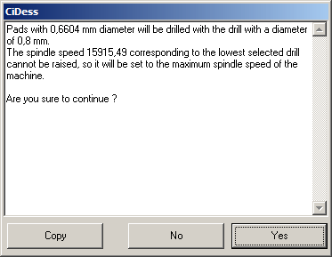
If some parameters cannot fit with your machine, CiDess shows you a detailed message:
Fourth step consists to choose how the PCB will be fixed on the machine:

With 1 to 4 choices, you have to locate the coordinate system with the mouse:

With choice n�5, you have to locate the origin of the coordinate system with the mouse and enter an angle:

With choice n�6, you have to select with mouse two reference points on screen, then fix the PCB on the machine, and thus locate the points with your CNC software:


With choice n�7, you have to select with mouse two reference pads on screen, then fix the PCB on the machine, and thus locate the pads with your CNC software:


Use your machine's software in 'JOG' mode to find first pad's location :


Use your machine's software in 'JOG' mode to find second pad's location :


CiDess shows you the measure error :

|
|
For a 4 inch PCB, a 1% error means a 0.04 inch hole location shift, it's too much. Error should be very small (as 0.2%). Put in spindle a thin drill or a needle and check it's not twisted. |
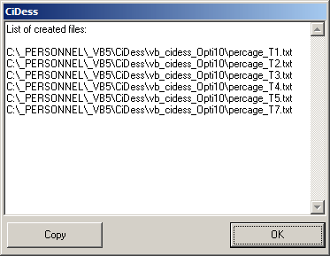
Last step is the GCODE files generation:

The textbox on the left explains you what you have to do with the files.
Now you can use GCODE txt files with your CNC machine's software :
|
|
� How to adjust HTool and Z G54� � buttons explains you how to put and measure tools on the machine, according to previous settings:
|

Here is an example :
After mounting a tool, set up your machine in 'JOG' mode and gently descend the spindle until the end of the tool touch the PCB :

In your machine's software select the spindle axis coordinate in the workpiece offset (here, Z in G54), and use the 'Measure' function :


Then, you can check that after measure, Workpiece Z is equal to 0, while the end of the tool is on the PCB :

So you can run the current tool GCODE program.
Do the same for each tool.
|
|
Add component types file in CiDess - CIT Files |
|
CiDess allows you to create your own component types. (see also component types editor). There are stored in CIT files.
If you read a CID file and if the author used his component types, an error will be occur: CiDess ask you for the CIT file.
There are two ways to read a CIT file:
- Move the CIT file in CiDess.exe path, quit and restart CiDess. Indeed, CiDess loads automatically all CIT files in CiDess.exe path.
- Load manually the CIT file; in "File" menu choose "Add a component type file...". Thus, you have to read again the CID file.
|
|
|
If a CID file reading trigs an error, it's important to read again the CID file after added all CIT files required.
In fact, after the first reading, components that have unknown component type are not loaded, so the PCB is incomplete.
|
|
|
New in version 2 (12/09/2005):
- if you add CIT files in CiDess.EXE path,
- if you edit a CIT file with the component types editor,
instead of restarting CiDess, use the "Refresh CIT files..." in the file menu.
Thus, all CIT files in CiDess.EXE path and all the CIT files manually added previously will be updated.
|
|
|
New in version 2 (12/09/2005):
If you have trouble to find a CIT file in your computer, go in file menu and launch the CIT files manager.
|
|
Run CiDess.exe with command line parameters
|
|
You can run CiDess.exe with command line arguments:
The three following command lines are doing the same:
cidess.exe chaudiere.cid siemens.cit "jack 6.35.cit" "power ics.cit"
cidess.exe siemens.cit "jack 6.35.cit" chaudiere.cid "power ics.cit"
cidess.exe /open chaudiere.cid siemens.cit "jack 6.35.cit" "power ics.cit"
Filenames with spaces may be in quotes "". The order you enter .CID and .CIT files doesn't matter; all .CIT files are read before the .CID file.
If you enter more than one .CID file, the first file is read:
cidess.exe siemens.cit chaudiere.cid emetteur.cid "jack 6.35.cit" "power ics.cit"
is doing the same than:
cidess.exe siemens.cit chaudiere.cid "jack 6.35.cit" "power ics.cit"
With /open_nocit command, CiDess will read only the .CIT files you enter in command line, not .CIT files in cidess.exe path:
cidess.exe /open_nocit chaudiere.cid siemens.cit "jack 6.35.cit" "power ics.cit"
|
|
Limit CiDess display area on screen
|
|
The III version allows you to choose how CiDess covers the screen. Go to display menu - > display area on screen...
The next window appears:

With default choice, CiDess will occupy the maximum space available by taking into account Windows start menu and toolbars (CiDess is now OK with Vista toolbars).
You can also define a custom display area:

Indeed, a new LCD screen is a little big, it will be more practical to share it in order to have several software simultaneously visible.
This option acts on the way CiDess displays windows after loading (first use while CiDess runs). If you maximize, re-size or move a window, it will keep its position and its size.
|
CiDess file manager allows you to find and sort easily the CIT files in your hard drive.
In "File" menu choose "Launch CIT files manager..."
The next window will appear:

You can choose a path and enter search parameters.
Clic on "Search" bouton to start search procedure.
|
|
|
Search procedure run time depends on the specified path. CiDess can't browse a 120Go HDD in 2 seconds!
|
Then the results will appear.
If you clic on a line of the table, a popup menu proposes you to open the CIT file in CiDess (= add the component types) or to localize the file with Windows Explorer.

With the file manager, you will never lose your files again!
|
CiDess file manager allows you to find and sort easily the CID files in your hard drive.
In "File" menu choose "Launch files manager..."
The next window will appear.
You can choose a path and enter search parameters.
Clic on "Search" bouton to start search procedure.
|
|
|
Search procedure run time depends on the specified path. CiDess can't browse a 120Go HDD in 2 seconds!
|
Then the results will appear:
|
CID files are sorted by project name and circuit name.
If you clic on a line of the table, a popup menu proposes you to open the file in CiDess or to localize the file with Windows Explorer.

With the file manager, you will never lose your files again!
|
|
Automatic HTML page generation
|
|
You create electronic devices and publish them on Internet? The automatic web page generation feature will save a lot of your time!
Once you have finished a PCB and fill all circuit information windows entries, save your file and in the "File" menu choose "Create HTML documentation...".
The next window will appear:

Select the data to publish and clic on "Next" button:

If you are created a schematic with another software, you can include it.
Clic on "Next" button:

You can publish the nomenclature.
Clic on "Next" button:

You can set up PCB picture parameters.
Clic on "Next" button:

You can set up layout picture parameters. You can add other pictures (for example case mounting instructions).
Clic on "Next" button:

You can include files to download.
CiDess allows you to save pictures as BMP files instead of GIF files. So you can use 3rd party software to convert BMP files to GIF. It's useful if you meet problems with CiDess' GIF files on your computer.
Now choose a name and a path for the HTML page and clic on "Finish" button.
Clic on "Next" button:

Wait a moment, a web page that describes your PCB is created!
Clic here to view an example.
|
CiDess allows you to create your own component types.
|
|
|
CiDess has a high number of component, sockets and heat sinks featured. But several users send me their "homemade"
CIT files with component types that already exist in CiDess. Before to use CiDess, take a moment to browse CiDess' component type's category.
A component type's name corresponds to a case, not to a component ref! for example. if you want to add a 7805 regulator in you PCB, go in "Standing
actives 3 pins" and choose "ISO220". When you browse CiDess' component types, CiDess show you a 3D preview to make things easy for you.
|

The window is divided into three parts.
First, the general purpose part:

 | "New" button creates and add a new component type. Next window will appear: |

 | "Change" button allows you to change ID and Category |
 | "Delete" button remove the current component type |
 | 50 mil left movement of the whole component |
 | 50 mil right movement of the whole component |
 | 50 mil back movement of the whole component |
 | 50 mil top movement of the whole component |
 | 50 mil bottom movement of the whole component |
 | 50 mil front movement of the whole component |
 | Flip |
 | Mirror |
In the middle, the pad part:

| Add a pad |
| Remove a pad |
| 50 mil left movement of the current pad |
| 50 mil right movement of the current pad |
| 50 mil back movement of the current pad |
| 50 mil top movement of the current pad |
 | Decrease current pad diameter |
 | Increase current pad diameter |
 | Decrease current pad's hole diameter |
 | Decrease current pad's hole diameter |
 | Add or remove a pin on a current pad |
 | Clic on this area to choose current pad shape. Next window will appear: |

At the bottom, the solid part:

| Add a solid |
| Remove a solid |
| 50 mil left movement of the current solid |
| 50 mil right movement of the current solid |
| 50 mil back movement of the current solid |
| 50 mil top movement of the current solid |
| 50 mil bottom movement of the current solid |
| 50 mil front movement of the current solid |
 | 15� rotation of the current solid |
 | 15� reverse rotation of the current solid |
| Clic on this area to choose current solid shape. Next window will appear: |

 | Clic on this area to choose the color used in 3D view. Next window will appear: |

Component type sample
|
Stretchable component type sample
|

Import components types from CiDess
In the "Edit" menu choose "Import a component type from CiDess...".
The next window will appear:
|

|
|
Use this function if you want to create another version of an existing component type.
|
Bilingual editing French - English
To activate bilingual editing, in "Edit" menu and choose "Bilingual editing".
Also you do not have to create bilingual component type.
If the "Bilingual edition" menu isn't checked, you access only to the ID and category in the current language. The component types created or modified are monolingual; in other words, French and English ID are the same, and so to the category.
|
|
|
To avoid confusion, don't mix bilingual and monolingual component types in a *.CIT file.
That is to say, do not translate partially a *.CIT file.
|
CIT files use in CiDess
There are two ways to read a CIT file:
- Move the CIT file in CiDess.exe path, quit and restart CiDess. Indeed, CiDess loads automatically all CIT files in CiDess.exe path.
- Load manually the CIT file; in "File" menu choose "Add a component type file...". Thus, you have to read again the CID file.
To avoid conflicts between CIT component types and CiDess featured component types, CiDess add "_" character to each ID of CIT component types.
|
|
|
New in version 2 (12/09/2005):
- if you add CIT files in CiDess.EXE path,
- if you edit a CIT file with the component types editor,
instead of restarting CiDess, use the "Refresh CIT files..." in the file menu of CiDess main window.
Thus, all CIT files in CiDess.EXE path and all the CIT files manually added previously will be updated.
|
CiDess allows you to view your PCB in 3D.
As I said in programmers' page, I created this function for educational purpose. If you want a good 3D view of your PCB, save it as STL or 3DG file and use a 3D software.
In the "Display" menu choose "3D view...".
The 3D utility will appear:

You can set up all 3D view parameters.
Clic on "Draw" button:

CiDess 3D utility allows you to control the picture with mouse.
|
CiDess allows you to add planar components, that is to say components made only with copper and epoxy:
- resistors
- selfs
- capacitors
Planar resistors:
In "Macro" menu, choose "Resistor track..."
The following window will appear:

You can set resistor's value, its shape and various parameters.
|
|
|
You have to enter PCB copper thickness. If you use a PCB width other copper thickness, the resistor's value will be different.
Also, do not tin the track corresponding to the resistor.
|
If values entered are badly scaled, CiDess prompts a detailed error message.
If values are OK, a track will appear, you have just to place it:

Planar self:
In "Macro" menu, choose "Self track..."
The following window will appear:

You can enter inductance value and its maximum resistance.
|
|
|
You have to enter PCB copper thickness. If you use a PCB width other copper thickness, the self's resistance value will be different.
Also, do not tin the track corresponding to the self.
Planar self calculation is complex and kindly imprecise; so if your application needs precise self value, you should made several prototypes to
measure exact value.
|
If values entered are badly scaled, CiDess prompts a detailed error message.
If values are OK, CiDess show you L and R value and a track will appear, you have just to place it:


Planar capacitor:
In "Macro" menu, choose "Capacitor track..."
The following window will appear:

You can set capacitor's value, and shape parameters. You must use a double-sided PCB.
|
|
|
You have to enter PCB thickness and its relative permittivity. If you use another type of PCB, capacitor's value will be wrong.
|
If values entered are badly scaled, CiDess prompts a detailed error message.
If values are OK, a track will appear, you have just to place it:

|
|
|
If you want to cancel a planar component just after you're clic OK, place the component anywhere on the circuit
and use undo function to delete it. You can also delete planar component's tracks later.
|
(c) Rémy LUCAS - Last update: 29/09/2018 (V4.29) |
|


